
EXPLORE THE NEW TRENDS AND ADVANCED TECHNOLOGIES IN THE HEAT TREATMENT EQUIPMENT INDUSTRY
Ask for a free consultation Ask for technical support

Tel

WhatsApp/WeChat
Contact Us
All products are customizable, leave message immediately, we will reply as soon as possible.
For your custom heating needs, reach us here:
CVD (Chemical Vapor Deposition) is widely used in the semiconductor industry, and the following are the main aspects of its application:

The Application of CVD in the Semiconductor Industry
Optoelectronic device manufacturing:
Photovoltaic cells: CVD is used to manufacture thin film solar cells, such as silicon films and compound semiconductor films (such as CdTe and CIGS), to improve photovoltaic conversion efficiency.
LED and Laser: This technology is used for depositing gallium nitride (GaN) and other III-V compound semiconductors to manufacture durable light-emitting diodes (LEDs) and lasers.
Hard mask in photolithography process:
CVD is used for depositing hard mask layers such as silicon nitride (Si ₂ N ₄) and silicon oxide (SiO ₂), which provide high-resolution pattern transfer and etching protection in lithography processes.
Gas sensor:
For example, metal oxide semiconductor gas sensors achieve high sensitivity detection by depositing sensitive films through CVD.
Excellent packaging:
Through Silicon Through Holes (TSV): CVD is used to deposit high-quality insulation layers and metal filling materials, and to manufacture three-dimensional integrated circuits (3D ICs) interconnection through TSV. Packaging protective layer: used for depositing protective layers to improve packaging reliability and durability.
Barrier layer and lining layer: Barrier layer deposition, such as titanium nitride (TiN) and tantalum nitride (TaN), serves as diffusion barriers for copper interconnects to prevent metal diffusion. Backing layer deposition is used to improve interface quality, improve the uniformity and adhesion of subsequent film deposition.
Optical applications:
The application of CVD diamond in the optical field includes windows for outputting heavy IR radiation from lasers, terahertz, and synchrotron radiation, as well as the manufacturing of refractive X-ray lenses.

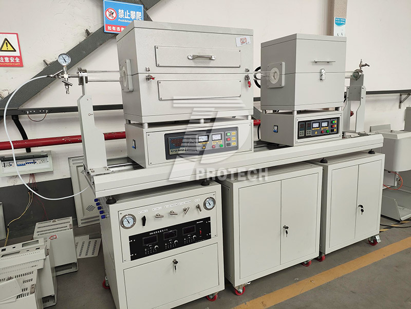
A commonly used slide CVD tube furnace (click on the image to view product details)
electronic product:
Diamond is used as a heat dissipation substrate and coating in the production of broadband semiconductor based devices. The use of "GaN Diamond" heterostructures can create a new generation of micro and high-energy efficient high-power microwave electronics, amplifiers, LEDs, and other electronic devices, especially those necessary for 5G network infrastructure.
Preparation of nanomaterials:
CVD technology can also be used to grow various nanomaterials, such as carbon nanotubes, graphene, etc. These nanomaterials have excellent mechanical, electrical, and thermal properties and are widely used in fields such as sensors and energy storage materials.
Semiconductor device manufacturing:
CVD technology is widely used in semiconductor device manufacturing, including materials such as grown silicon, alumina, silicon nitride, silicon carbide, and phosphide. Among them, monocrystalline silicon and polycrystalline silicon are the main applications of CVD technology in semiconductor device manufacturing.
In addition, CVD silicon carbide components have been widely used in multiple fields due to their unique performance advantages, especially in etching equipment, MOCVD equipment, Si epitaxial equipment, SiC epitaxial equipment, and rapid heat treatment equipment, all of which play a very important role.

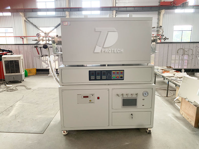
Customized three temperature zone CVD tube furnace (click on the image to view product details)
Overall, the application of CVD in the semiconductor industry covers all aspects from basic material preparation to high-end equipment manufacturing, making CVD widely used in the semiconductor industry.Click to learn more CVD devices! Or click on online customer service to learn more about product information!